Our services

Foundry Link Service Offerings

Design Enablement

  • Access to EDA/CAD Tools
  • Access to Foundry PDK
  • Design Service (RFIC & RFSOI)

Fab Service

  • Multi Project Wafer (MPW) Prototype Run Service
  • Multi-layer Mask (MLM) / Full MasksetEngineering Run Service
  • Low to High Volume Production

Backend Service

  • Wafer Back Grinding / Dicing
  • Die sort for pick and place
  • Wafer BUMP
  • Broad Assembly (QFN, QFP, COB, WLCSP, FCBGA)
  • Air Cavity Specialty Packaging (ACP RQFN)
  • Wafer Test / Package Test / Module Test
  • Failure Analysis & Reliability
  • PCB / PCBA

MPW Service Offering

  • MEDsMPW Service help accelerate your ideas into reality, focusing on 350nm to 12nm specialty CMOS & III-V pHEMT/HBT technology

Foundry Service Offerings

  • Bulk CMOS
  • BCD & BCDLite®
  • FDX™ FD-SOI
  • FinFET 12LP+
  • RF SOI
  • SiGe
  • Gallium Nitride (GaN)
  • Silicon Photonics
  • ams-OSRAM Technology portfolio

Backend Service

  • Wafer Back Grinding / Dicing
  • Die sort for pick and place
  • Assembly (DIP, SIC, QFN, QFP, COB)
  • Air Cavity Specialty Packaging (ACP RQFN)
  • Failure Analysis & Reliability
  • PCB / PCBA
Years
Experience
+ 0

FIND OUT MORE

Wafer services

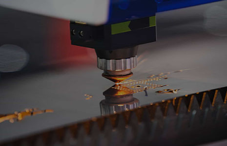
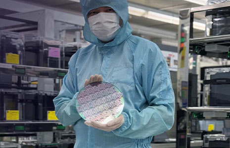
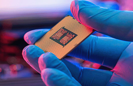
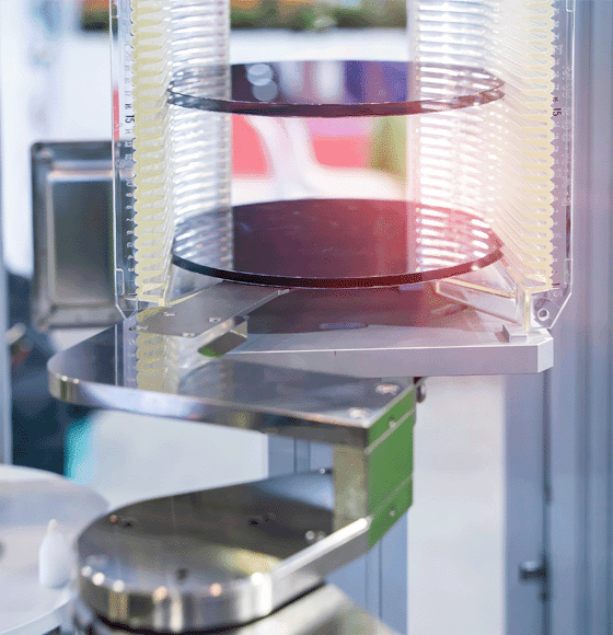
As a part of a full turnkey offering, FLS offers Bump, Wafer Level Package and Probe capabilities, complemented by OSAT partnerships, to provide a one-stop-shop for customers’ wafer needs. Creating a reliable and high-quality path to production, FLS streamlines manufacturing so customers can realize their designs quicker.

  • Bump offerings for 200mm and 300mm, including SnAg bump, copper pillar and WLCSP
  • Wafer sort with Known-Good-Die methodology
  • Backside grind, wafer sort and bake, dicing, marking and binning services available